2.4 GHz Inverted F Antenna Eagle Library
2012/05/06 16 Comments
ISM radios for microcontroller are becoming quite popular in last years, and if you are designing with wireless radios you have a wide choice of transceiver in both sub-gigahertz an 2.4 GHz bandwidth.
If you choose to go for 2.4 GHz, you’ll have the benefits of a wide choice of radios, relaxed constraints in protocol design and a small size antenna.
Focusing on the antenna, 2.4 GHz radios usually have a differential output which have to be adapted to a 50 Ohm single-ended signal suitable for Wi-Fi antennas, which can be connected to the radio using an RP-SMA connector or directly embedded into the PCB.
This post shows a printed antenna design, kindly provided by TI/Chipcon, suitable for 2.4 GHz ISM radios. You’ll also find a link for an Eagle library with some tuning variant.

2.4 GHz Transceivers
All major microcontroller manufacturer provides radio-enable MCU or external radios. Using an external SPI-driven radio simplify software design, as you can reuse the same code on nodes with different architectures, creating a mix of nodes using microcontroller, SoC and standard PCs.
Most 2.4 GHz radios are designed for use with IEEE 802.15.4 stacks (including ZigBee and 6LoWPAN) but others are explicitly designed to simplify the implementation of a custom stack (like the Nordic nRF24 series).
Independently of the radio chip, if you are using a general purpose 2.4 GHz antenna, you have to include the hardware necessary to adapt the output of the radio to a single-ended 50 Ohm line as specified by device’s datasheet. That’s what every external antenna and most printed antennas use.

Antenna designs
2.4 GHz signals imply a quarter-wave of about 31mm (that’s 1.22 inches for you, imperial friends), so that’s going to be about the major size of most unfolded printed antennas, like the one showed in this post. If your design has tighter size constraints look for a folded-design, which is what is commonly used in usb-keys.
When using a printed antenna, you have to be sure that the design matches your board stackup – or is stackup-independent at all. That can be a problem as most dual-layer printed antennas are designed for thin stackups, while hobbyist PCBs are usually standard 1.6mm thick.
One of the better place to get free information about printed antenna designs is the Application Note section of TI’s website. Here you’ll find some really good design for both a folded and unfolded antenna and a comparrison chart of all their antenna designs.
TI/Chipcon IFA (Inverted F Antenna)
This is an implementation of TI’s Inverted F Antenna (DN007) which I’m currently using with an AVR-driven Nordic nRF24L01+ general-purpose radio.


The symbol is provided with the main element tunable from the suggested design from -3mm to +5mm. That’s because tuning is influenced by many external factors, and have to be done with the antenna in the working environment to be correct.
Fot further details, see the original application note: DN007.
Tuning
Antenna tuning is really easy, <irony>you just need a friend with a network analyzer capable of doing SWR analysis!</irony>
If you have that, you probably already know what to do: just design the board with the longer variant of the antenna, connect the analyzer and cut down the antenna until the natural resonance matches the desired range, usually 2.4 to 2.5 GHz. The easiest way to strip the antenna is to remove some of the solder mask, slice out the part to be removed, and then heat up the excess copper using a solder iron until it detach itself from the PCB.
In my design, I had to cut the antenna down to the -2 marker.
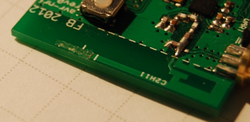
That’s how the cut antenna looks like. You can see from the picture that the layout provide a path from the antenna feed point to an RP-SMA connector, used for tuning.
If you don’t have such instrumentation available, it’s probably better to just use the default tuning (the +0 variant).
Eagle Library
The eagle library is part of a board I designed recently to test the Nordic radio transceiver. You can find the lbr file with just the antenna here.

The layout has been tuned to pass BatchPCB DRC bot, so you can easily use this design with low-cost PCB manufacturing services.
Further Resources
TI probably has the best free application notes for printed antenna design, including also some differential layout which requires no matching network for their CC-series chips. Just point to the page of one of their 2.4 GHz product and grab all the PDFs you can.
Nordic Semiconductor also has an antenna design guide, which is really basic, but is worth reading anyway.


I notice that your matching network looks like a bunch of caps, rather than an SMD balun or the like. Can you comment a bit on how that works? Also, is the board designed to be jumper switchable between the external and printed antennas?
Hi Pierce,
you’re right, there are a lot of passive components for the matching network, including capacitors and RF chokes. The reason why I used that circuit instead of a balun is just because I re-used the components from a pre-assembled breakout board of the chip. Those are easier to find on ebay and have an overall cost much lower than the IC and a balun from distributors.
About the design, that’s implemented 1:1 from chip’s datasheet (chapter 11 – application example).
About the SMD balun, Nordic provides an application note with the part number of a compatible balun (Johanson 2450BM14A0002), but that’s even harder to obtain and maybe quite difficult to hand-solder.
As for the switch, I just added two SMD pads to be soldered together. A common jumper on a 2.4GHz signal doesn’t sound like a really good idea… But an RF switch would be great! Just hard to find on eBay :-)
Anyway, this post was just meant to show TI’s printed antenna. I’ll try to cover the whole ATMega32U2 + nRF24L01p circuit/firmware on another post.
Thanks for the comment!
Hey, just wanted to thank you for your eagle design :)
I am not an antenna engineer either, but I am currently doing a few breakout boards for the AT86RF231 chip (fur fun, not for profit) where I want to compare a few different antenna designs (TI’s meander and inverted f, a wire lambda/4 and a chip antenna). I originally didn’t want to include the F-antenna, because it’s really big, but when it’s that easy, why not? If you want I’ll let you know how it goes.
I have also did some work with the Nordic chip in the past, may I ask why you go through all the trouble of designing your own RF circuitry, when you can just buy those awesomely cheap breakout-boards on the net based on Nordic’s reference design?
Hi Chris,
I agree that inverted-F is quite big, but unless you are designing an USB key-sized PCB, it should be a decent compromise… also I think it looks cooler than meander for what it matters! :P
As for the breakout, I actually brought some awesomely cheap breakout-board based on Nordic reference and than recycled the components to mount my board (hot-air rules here). I see that that’s actually a bit crazy, but I also wanted to compare the antenna design (a meander on breakout i brought, the inverted-F and external antennas like dipole or waveguide on SMA).
No problem for the eagle library, share a link if you publish your test results – I’m very interested in that (I’m doing it for fun either)!
I’m also looking forward to some AT86RFxxx-based design, they looks really good on the paper, but seems to be quite complicated to use without any external 802.15.4 library. Are you using a custom stack?
Fabio
So, how did the Nordic design do compared to the F-antenna?
Actually i chose the AT86RF because it seems really well supported. There is code (and a whole thoroughly tested 6LoWPAN stack) in Contiki, which has already been ported to AVR. There’s also a Linux driver for it in the Linux-Zigbee project.
I’ll publish it here: http://blog.flokati.tk/ The AT86RF board will be pin-compatible to the NRF board, so I can put it in my protoboards.
I did not run any serious test yet, but at first sight inverted-F and the meander i had on the breakouts (they looked the same as the one on your blog!) seem to perform quite similarly, while an external dipole (a standard wifi antenna) on SMA is a bit better (read: reach some spot better but nothing *that* special).
I’ll try the nordic with my wifi cantenna if I’ll ever find some time and place to do that! :)
Contiki looks like good stuff, and I like the idea of doing something with 6LoWPAN in the future. Still, I think it requries a pretty big microcontroller, while with the nordic you can do some neat stuff with just a ‘tiny!
For linux-zigbee, I see that some part of the patches are being integrated into mainline… that may be a reason to get some AT89* radio by itself!!
I’m also following this project http://en.qi-hardware.com/wiki/Ben_WPAN, they have a linux-zigbee driver and full hw/sw/fw source for an USB-to-AT89something with a really clean USB stack.
Cheers!
Can i go with this IFA antenna design in my nRF51822 BLE module design?
Hey Dharm, sure thing, this worked great for me in different 24l01+ designs, it should be fine with anything in the 2.4GHz band that has a 50 Ohm matching (such as all baluns linked in the device website).
Hi,
Thank you for reply,
Can you help me out in layout as i am confused,
Silicon LAbs says to not use pouring on top layer while texas has used top layer pouring.
I have used stack layer as follow, pls share your feedback:
1) RF routing + Poured GND plan
2) Ground Plan
3) Power Plan
4) Ground plan
where in design all vias connect to both ground plan(Layer 2 and Layer 4).
Well I think the TI design is filled because it’s on a two layer PCB. If you use a four layer stackup you are probably going for a thin prepreg between layer 1 and 2 right? In that case I would guess that you should just remove the filling below the antenna (as by TI application note) and it’s probably going to perform in the same way. That’s a best guess though – I don’t actually know much of RF and don’t have any RF Engineer at beer range anymore. :-)
What is the recommended dielectric for 2 layer PCB to use this IFA PCB antenna. I would be more helpful if you can provide complete 2 layer PCB stack up for using this IFA PCB antenna
Does it matter? The opposite layer is empty…
Checking the original application note (http://www.ti.com/lit/an/swru120c/swru120c.pdf):
Because there is no ground plane beneath the antenna, the PCB thickness will have little effect on the performance. The results presented in this document are based on an antenna implemented on a PCB with a 1-mm thickness.
The one on the picture is on a standard 1.6mm FR4.
iam unable to download the library file..if i click the link it opens a page with programing code..how do i execute it
Use right click, “save link as”.
actually i did..i saved as notepad file..is that right way to do.
actually i did..i saved as notepad file..is that right way to do.