Power Manager: Soft Power Control of USB and Low Voltage Devices
2013/03/22 10 Comments
One frustrating aspect of firmware or kernel development on commodity hardware, such as cheap evaluation board or production devices, is the necessity of power-cycling the target device to reboot it every time the developer needs to load and run a new software build.
It sometimes happens that a development board is designed with proper management electronics to ease software development or automated testing, but in most cases the developer has reset the board manually, and sadly quite often reset buttons are unaccessible or just non-existent, requiring the developer to unplug and replug the power cable. If this ends up in your workflow and at the end of the day your fingers hurt, something is wrong.
This project is a small AVR/V-USB based board to control the power supply of development boards and other low voltage and USB powered devices. It allows to program a sequence of events for the output ports, has LED indicators for port status, and additionally provides power measurement on both USB and main power channels, and uses a bootloader for easy firmware upgrade… All in a solid and funny looking Hammond blue box!


Main Microcontroller
The brain of the board is the usual ATmega168 microcontroller, powered from the “control” USB port at 3.3V with a linear regulator, and clocked at 12MHz.
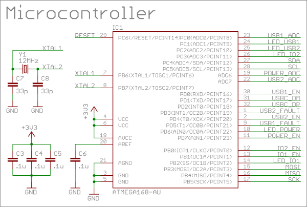

The firmware is based on the V-USB library to provide easy host connectivity. The protocol is designed as a vendor specific USB device, with just some custom control requests to enqueue events, clear the queue, query the status and reset the device. Use the source!
Bootloader
The microcontroller implements a customized version of bootloadHID from obdev.at. The bootloader uses the control USB port, and is modified to run for some seconds every time the microcontroller exits from reset.
This means that to upgrade the board firmware, the only operation to do is to issue a reset command, or power cycle the board itself if the current firmware is broken… So, the board itself is unbrickable, and allows automated firmware upgrade as long as you don’t upload a completely broken firmware!
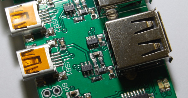
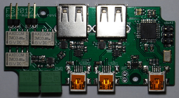
USB Ports
The two USB channels (usb1 and usb2) have two couples of mini-USB to USB host ports, with straight-through data and common ground.

The USB supply line of each port goes trough a TPS2552 precision adjustable power distribution switch. The TPS provides configurable (via resistor) overcurrent protection and power control.
Additionally, each power line has a shunt resitor connected to an INA219, an I2C bidirectional current and power monitor, that provides power consumption information to the microcontroller.
The power monitor is useful to debug battery charging algorithms or to profile the power consumption of an USB device.
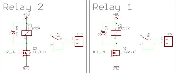
Main Power Port
An additional power line using terminal block connectors allows to control a generic power supply line for the target board. The limitation is the absolute maximum voltage of the INA219, and that is 26V, and the fact that the negative terminals are connected together with USB ground and shielding.
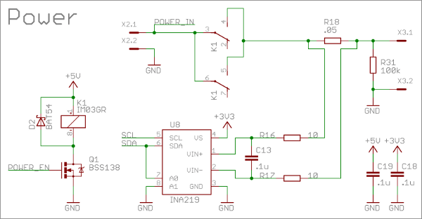
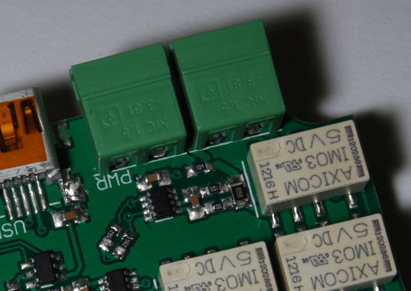
The generic power line uses a small TE SMD relay, rated for a current of up to 2A per contact. The two contacts are wired in parallel, and eventually a high current version of the same relay is available.
Again, a shunt resistor and an INA219 are used to provide power consumption measurement.
An interesting alternative usage for this port would be to connect a battery instead of a normal power supply. As the INA219 is bidirectional, that would allow to measure the whole charge/discharge curve of the system.
Additional I/O
If you are really REALLY unlucky, your development board requires you to close a jumper or press a button to enter some kind of “programming mode”, or simply to turn it on.
In this case, you should really complain to the hardware engineer who designed it, but this is not always possible, so the two additional I/O channels (io1 and io2) have an isolated output that just shorts when active, and can be used to simulate the pressure of a switch, or just as an additional power line.

Box
This kind of circuits are usually used in a mess of tangled cables and other bare boards, and is not going to survive for long without a proper box.

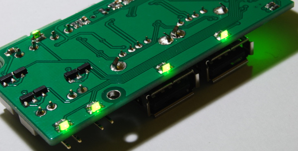
So, the PCB fits nicely in an Hammond 1551K Box, and if you buy the translucent version (marked as 1551KTBU), you will be able to se the status LEDs on top and under each port… Nice!


Firmware Operation
The firmware is quite simple, and the most important thing is an USB CUSTOM_RQ_EV_PUSH control request to enqueue events on a queue periodically processed in the main microcontroller idle-loop. A dedicated timer is configured to give precise delay, and each event can be specified to be delayed from the precedent, allowing to program complex power on/off sequences.
The other important thing is the CUSTOM_RQ_STATUS control request to read the output statues, and the instant power consumption from the INA219 ICs.
Control Application
The userspace application is a libusb based application (named pm), that is easy to script and allows to control all the features of the device, including printing the actual status.
That’s the syntax help of the application:
$ pm -h
Usage: pm -h
       pm -R
       pm [options]
options:
  -h         this help
  -R         reset device
  -s         show status
  -w         wait delay in tenth of seconds
  -C         clear event queue
  -e list    enable listed i/o (comma separated)
  -d list    disable listed i/o (comma separated)

valid i/o: usb1,usb2,power,io1,io2,all
And this is an example of the status output:
$ pm -s
              USB1*  USB2  POWER*   IO1    IO2
 voltage_in:   5161      0   4130
voltage_out:   5148    920   4172
    current:      1      1    203
      power:      0      0    860
       fail: 00
Complex events can be programmed by calling pm for each event, specifying a delay for each one using the -w flag and a number in tenths of seconds, as in:
# turn everything off
pm -d all
# enable usb and power after 1/2 second
pm -w 50 -e usb2,power
# turn usb2 off after 6 seconds
pm -w 600 -d usb2
# turn usb2 back on after 1/2 second
pm -w 50 -e usb2
That’s it! No complex operation and easy port mnemonic!

Design Files
As always, you can download the hardware and firmware files for this design from GitHub.

The schematics in PDF version can be downloaded from here.


Hello Fabio,
What version of Eagle have you used for your power manager design?
Thanks,
Ross
Hi Ross,
I’m using Eagle 6.4 (it should be the latest available), the design is well within the freeware license!
Fabio
Thanks Fabio.
I am still using 5.4 because of my library collection. I guess I will have to upgrade.
Cheers,
Ross
Well, since v6.0 all eagle files are in XML format, and that’s a *big win* for version control… On the other side 6.4.0 currently has some unfixed bug – it resets some custom shortcuts on start, so you may want to get 6.3 if you need that.
You libraries would just get updated to the new format on save, so you will loose compatibility with older version… It’s up to you!
Fabio
Reblogged this on Byte Outa Life and commented:
Wow, what an incredible project! So well put together. I’m truly impressed.
Whoa, thanks! :-)
Fabio,
When you were choosing the parts for your design, did you consider the INA3221 instead of three INA219 devices?
Cheers,
Ross
Not really… I’m not even sure it was available when I discovered the INA219.
Actually it looks nice! I like the QFN16 package and you save some money, but I think that the INA219 is easier to route on a 2 layer board. Also, the ‘219 is bidirectional, and that’s a cool feature for spotting strange power paths or battery charging/discharging.
Fabio
Hi, Not sure if you’re still maintaining these, but really good to know the technique you’ve been using for cutting your case holes for the ports – very tidy looking job and much neater than the ones i’ve done. Care to share your secret approach ?
Simon
Hey, thanks for the comment! :-) My standard strategy for cutting the holes is to first define the hole height by scribing the top and bottom lines with a caliper (the points are sharp and marks the plastic pretty well) using the top edge of the box, where the lid seals, as a reference — that’s the only flat part. I use a bare PCB as a reference to take the dimensions and for visual inspection. Then I try to guess the width of the hole visually (the box is semi-transparent), scribe that as well and drill a couple of undersized hole in the center (2/3mm). From there I expand the holes to the rectangular dimension with some jewellery files and by test-fitting from the deeper connector. Takes lot of patience, the secret is to get some groovy tune in the background. :-)
Lately I started using a small manual mill with a 2mm endmill. Same technique but less filing involved: I try to mill to the final dimension and only file the corners to get them square (i.e. remove the 2mm tool radius) and the top of the hole to put a bevel (to facilitate the board insertion from a side).
In either case the bevel part is very important, if you don’t get it right you may end up cutting the holes too high (because the board inserts at an angle) and end up with a gap in the top when the board lies flat. This is harder to get right when you have multiple connectors flush with the outer face of the box.
Good luck! :-)